 |
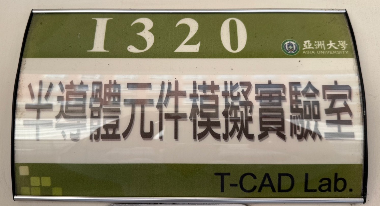
 - Semiconductor Device Simulation Laboratory (I320) - Equipped with semiconductor device simulation tools, this lab supports students in conducting simulations and analyses of semiconductor device characteristics.
|
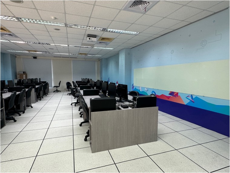
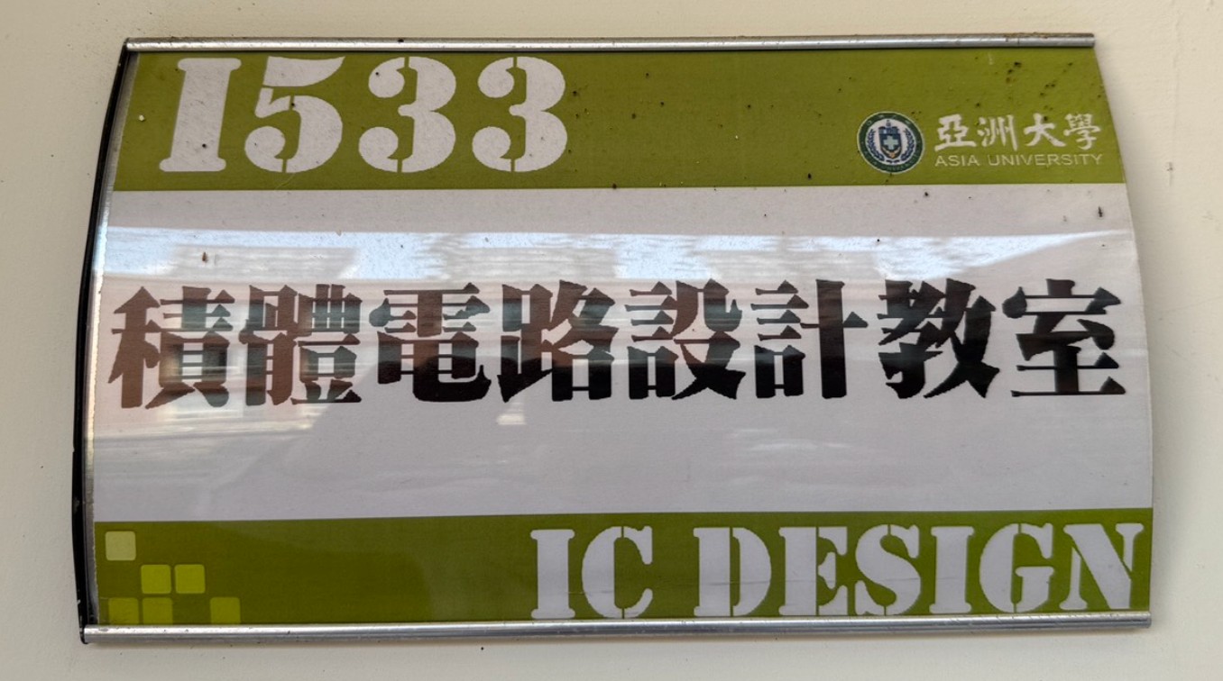
 - IC Design Laboratory (I533) - Specifically designed for IC design courses, this lab enables students to learn and practice the integrated circuit design process.
|
 |
 |
 -
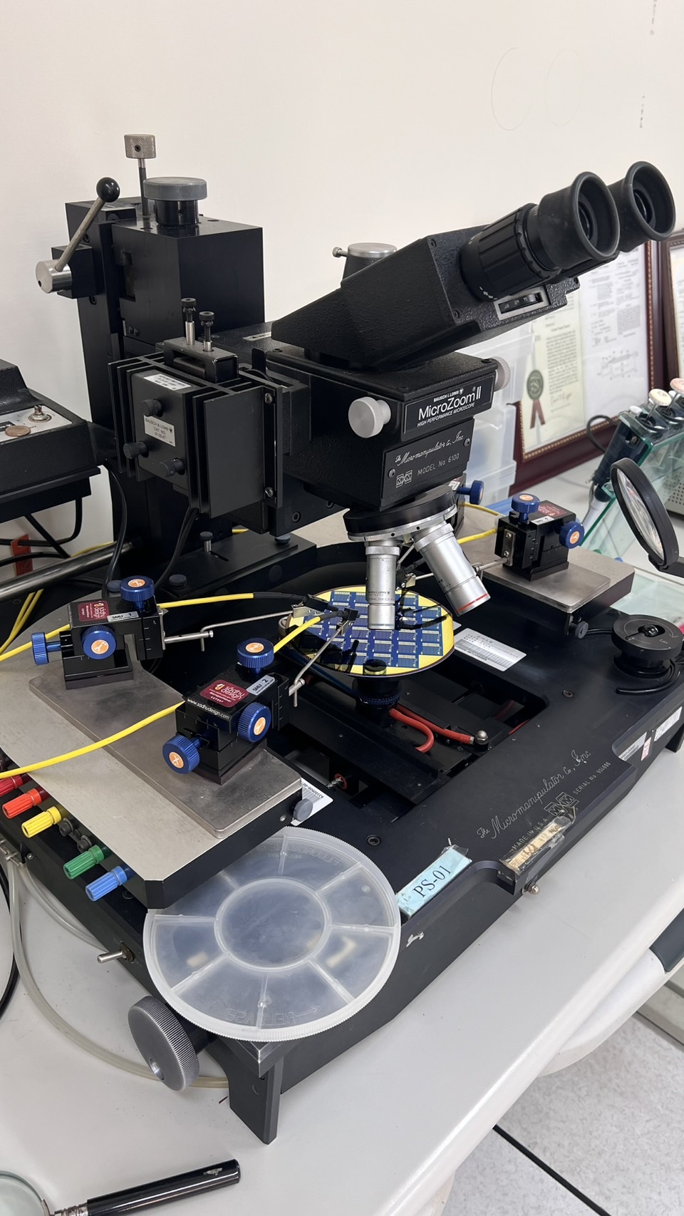
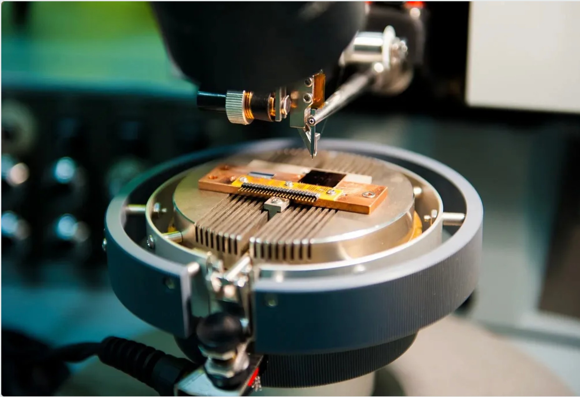
Semiconductor Testing Laboratory (I534) - Equipped with semiconductor testing machines that allow students to gain hands-on experience in semiconductor device testing and analysis. This lab provides data analysis and application software to support students in understanding failure mechanisms, circuit behavior, and performance evaluation. It plays a vital role in ensuring semiconductor device reliability by teaching students testing methodologies and quality control techniques used in the industry.
|
 - AMD Electronic Circuit Laboratory (I634) - Featuring professional equipment provided by AMD, this lab allows students to learn and apply advanced electronic circuit technologies.
|

|
 
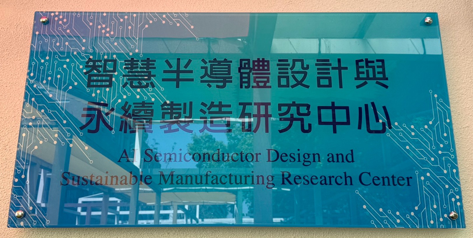
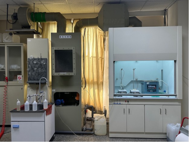
Intelligent Semiconductor Design Laboratory is a high-tech facility equipped with advanced semiconductor fabrication and characterization equipment. It provides students with hands-on experience in thin-film deposition, material analysis, and semiconductor process technology.
The lab includes the following major equipment:
This lab serves as a core facility for semiconductor material research and device prototyping, allowing students to gain practical experience in semiconductor manufacturing and process development.
|
 |
