

<style>
/* 1. Global Container: Magazine-width and font texture */
.magazine-container {
font-family: "Segoe UI", "Roboto", "Helvetica Neue", Arial, sans-serif; /* Professional English Fonts */
color: #2c3e50; /* Dark Grey-Blue */
line-height: 1.8; /* Golden ratio line height */
font-size: 16px;
max-width: 800px; /* Reading width limit */
margin: 0 auto; /* Center alignment */
padding: 20px;
background-color: #fff;
}
/* 2. Title Design */
.magazine-title {
color: #004085; /* Professional Deep Blue */
font-size: 26px;
font-weight: bold;
margin-bottom: 8px;
line-height: 1.3;
}
.magazine-subtitle {
font-size: 18px;
color: #555;
font-weight: normal;
margin-bottom: 25px;
padding-bottom: 20px;
border-bottom: 1px solid #eee; /* Divider */
}
/* 3. Section Headers: Left border style */
.section-header {
font-size: 20px;
font-weight: bold;
color: #0056b3;
margin-top: 40px;
margin-bottom: 15px;
padding-left: 12px;
border-left: 4px solid #0056b3; /* Blue accent */
}
/* 4. Highlight Text */
.highlight-text {
font-weight: bold;
color: #d63031; /* Accent Red */
}
/* 5. Image Module */
.magazine-figure {
margin: 35px 0; /* Vertical spacing */
text-align: center;
}
.magazine-figure img {
display: inline-block;
max-width: 100%; /* Responsive width */
height: auto;
border-radius: 6px; /* Rounded corners */
box-shadow: 0 4px 12px rgba(0,0,0,0.15); /* Lifted effect */
}
/* Caption Style */
.magazine-caption {
margin-top: 10px;
font-size: 14px;
color: #7f8c8d;
font-style: italic;
font-family: "Georgia", serif; /* Serif font for captions */
}
/* 6. Portrait Image Limit */
.portrait-img {
max-width: 400px !important;
}
/* Mobile Adjustment */
@media (max-width: 600px) {
.magazine-container { padding: 15px; }
.magazine-title { font-size: 22px; }
}
</style>
<div class="magazine-container">
<div class="magazine-title">Cross-Disciplinary Dialogue, Co-Creating the Future</div>
<div class="magazine-title" style="font-size: 22px;">Asia University Semiconductor Delegation Visits Global Equipment Leader Lam Research</div>
<div class="magazine-subtitle">
<strong>Focusing on Advanced Process Challenges and Deepening Industry-Academia Dialogue on Talent Cultivation</strong><br>
<span style="font-size: 14px; color: #888;">【February 6, 2026 | Hsinchu, Taiwan】</span>
</div>
<p>
To accurately grasp global semiconductor technology trends and talent development, Asia University Vice President <strong>Jun-Jie Huang</strong> led a delegation of semiconductor professors today (Feb. 6th) to visit the Taiwan headquarters of <strong>Lam Research</strong>, a global leader in semiconductor wafer fabrication equipment, located in the Hsinchu Science Park. The visit centered on the evolution of advanced process technologies, practical industry challenges, and semiconductor talent cultivation, exploring diverse possibilities for future industry-academia collaboration through in-depth dialogue.
</p>
<figure class="magazine-figure">
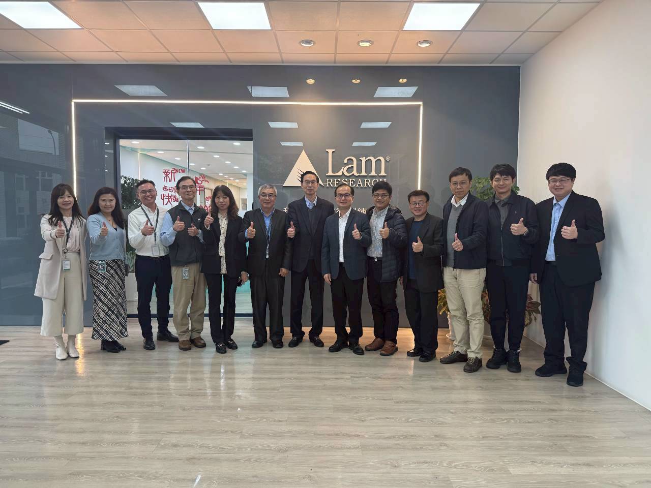
<img src="/uploads/asset/data/6985d1ce063ca2cb0f5da6d6/LINE_ALBUM_26_Lam_260206_1.jpg" alt="Asia University and Lam Research Team Photo">
<figcaption class="magazine-caption">▲ Team Synergy: The entire delegation poses in the lobby, symbolizing the positive interaction between the two institutions.</figcaption>
</figure>
<div class="section-header">Global Top 3 Equipment Supplier: Lam Research’s Critical Industry Role</div>
<p>
<strong>Lam Research</strong> is one of the world's top three suppliers of semiconductor wafer fabrication equipment, deeply rooted in critical <strong>Deposition</strong> and <strong>Etch</strong> technologies. As process nodes advance to 3nm and beyond, Lam's high-precision technologies, such as <strong>Atomic Layer Deposition (ALD)</strong> and <strong>Atomic Layer Etch (ALE)</strong>, have become essential for enhancing the structure and performance of advanced devices.
</p>
<p>
According to public information, Lam Research's equipment and solutions are widely used in the manufacturing of logic chips, memory, High-Performance Computing (HPC), and AI chips. With R&D and manufacturing centers located globally, Taiwan serves not only as a vital operational and technical support hub but also plays a key role in the global semiconductor supply chain.
</p>
<div class="section-header">Visit Record: Technical Exchange & Talent Dialogue</div>
<p>
The visit was centered on "Industry-Academia Sharing, Technical Exchange, and Talent Cultivation," covering corporate introductions, research capacity presentations, open forums, and a tour of training facilities.
</p>
<p>
<strong>14:00–14:20 | Corporate Introduction</strong><br>
The delegation was hosted by Lam Research Vice President <strong>C.T. Chiao</strong> and key executives. VP Chiao introduced Lam’s corporate history, global footprint, and the strategic role of the Taiwan site. He highlighted the company’s long-term investment in advanced process R&D and global service systems, providing the Asia University team with a clear understanding of how Lam maintains its leadership in the highly competitive equipment market.
</p>
<p>
<strong>14:20–14:40 | Asia University Research & Teaching Capacity</strong><br>
Vice President <strong>Jun-Jie Huang</strong> presented Asia University’s layout in semiconductor teaching and research. VP Huang emphasized that, with support from the <strong>Ministry of Education (MOE)</strong>, Asia University has established a "Semiconductor Bachelor’s Degree Program." Driven by industry needs, the program constructs an all-encompassing learning environment combining theory, practical training, and cross-disciplinary skills, aiming to cultivate "industry-ready" professionals.
</p>
<figure class="magazine-figure">
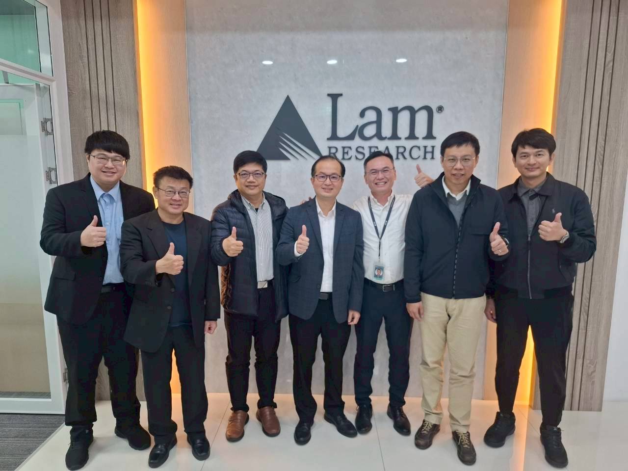
<img src="/uploads/asset/data/6985d24a063ca2cb0f5da6d9/LINE_ALBUM_26_Lam_260206_3.jpg" alt="VP Huang and Director Jason Kao">
<figcaption class="magazine-caption">▲ Witnessing Technical Exchange: VP Jun-Jie Huang and Director Jason Kao pose before the "Lam Research Taiwan Warmly Welcomes Asia University" signage.</figcaption>
</figure>
<p>
<strong>14:40–14:50 | Open Exchange Forum</strong><br>
During the open forum, the Asia University team—including Dean of General Affairs <strong>Chao-Nan Chen</strong>, Associate Professors <strong>Yu-Ming Peng</strong> and <strong>Jung-Hui Yeh</strong>, and Assistant Professors <strong>Ying-Jung Ho</strong> and <strong>Yun-Shao Cho</strong>—engaged in an in-depth discussion with <strong>Jason Kao</strong>, Director of the Advanced Technology Group. The dialogue focused on "pain points" in advanced processes, ranging from equipment requirements and process stability to how academic research can address real-world industry challenges.
</p>
<p>
Simultaneously, Senior HR Director <strong>Elaine Yang</strong> and Operation Director <strong>Anna Chou</strong> showed great interest in semiconductor talent development. They raised questions regarding talent sourcing and competency building. It was noted that Lam Research operates a <span class="highlight-text">significant manufacturing site in Taoyuan</span>. As the demand for advanced process equipment grows, the need for talent with strong engineering foundations and cross-disciplinary understanding is becoming increasingly urgent, making talent pipelines a core topic of the discussion.
</p>
<p>
<strong>14:50–15:30 | Asia Pacific Technical Training Center Tour</strong><br>
The visit concluded with a tour of the "Asia Pacific Technical Training Center," guided by Senior Manager <strong>Charle Liu</strong>, Consultant <strong>Jason Chang</strong>, and University Relations Manager <strong>Elly Chen</strong>. The team gained on-site insights into the rigorous systems a global equipment leader uses for engineer training, technical verification, and safety protocols.
</p>
<div class="section-header">Outlook: Deepening Exchange and Advancing Cooperation</div>
<p>
Regarding future internships and industry-academia collaboration, both parties exchanged constructive views on talent alignment and practical learning models. Asia University demonstrated its active layout in semiconductor education, while Lam Research shared insights on global industry demands. Both institutions expressed high expectations for deepening future interactions, hoping to explore concrete cooperation models that will inject long-term momentum into Taiwan's semiconductor talent pool.
</p>
<figure class="magazine-figure">
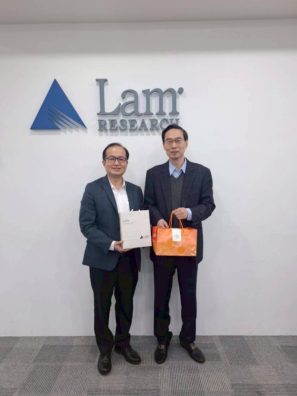
<img class="portrait-img" src="/uploads/asset/data/6985d1f3063ca2cc12fda5d9/LINE_ALBUM_26_Lam_260206_4.jpg" alt="VP Huang and VP C.T. Chiao">
<figcaption class="magazine-caption">▲ Strategic Vision: VP Jun-Jie Huang (left) and VP C.T. Chiao (right) showcase a shared vision for sustainable industry development.</figcaption>
</figure>
</div>
Login Bachelor Program of Semiconductor