View count:
229
Sputtering Systems
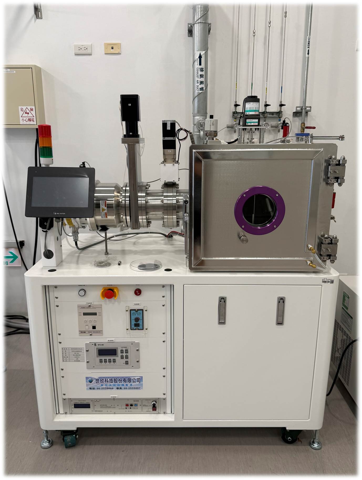
Sputtering Deposition System
Instrument Overview

Sputtering is a Physical Vapor Deposition (PVD) technique that uses Argon ions to bombard a target material. This kinetic energy knocks target atoms out, which then deposit onto a substrate to form a thin film. This technique allows for the fabrication of high-density, highly adherent thin films at relatively lower temperatures, and is commonly used in semiconductor, optoelectronic, and magnetic device manufacturing.
Key Applications and Functions
- Semiconductor Processing: Deposition of metal interconnects and electrode layers for chip conductivity and interconnection structures.
- Optoelectronic and Solar Components: Fabrication of transparent conductive layers, reflective layers, or absorption layers for photodetectors and solar cells.
- Magnetic Device Manufacturing: Production of magnetic thin films for data storage and sensing elements.
- Micro-Electro-Mechanical Systems (MEMS): Formation of conductive or protective layers to enhance the durability and conductivity of microstructures.
Working Principle
- Vacuum Chamber and Argon Introduction: The sample is placed in a vacuum chamber, and Argon gas is introduced to create a low-pressure environment.
- Plasma Generation: Applying voltage ionizes the Argon gas, creating Argon ions (Ar⁺) and electrons (Plasma).
- Target Sputtering: Argon ions, accelerated by the electric field, bombard the target surface, causing target atoms to be ejected and deposited onto the substrate.
- Thin Film Growth: Controlled heating and rotation of the substrate ensure uniform deposition and the formation of a dense film structure.
Comparison of DC and RF Sputtering Techniques
The table below compares the main characteristics and application differences between DC Sputtering (Direct Current) and RF Sputtering (Radio Frequency):
| Characteristic | DC Sputtering (Direct Current) | RF Sputtering (Radio Frequency) |
|---|---|---|
| Applicable Materials | Conductive metals (e.g., Cu, Al) | Conductive or non-conductive materials (e.g., oxides, nitrides) |
| Principle | DC electric field accelerates ions to bombard the target and eject atoms | RF electric field excites ions to bombard the target and release atoms |
| Deposition Rate | High | Relatively Lower |
| Film Uniformity & Quality | Uniform, good adhesion | High quality, controllable composition and density |
| Limitation | Cannot deposit non-conductive materials | Slower deposition rate |
| Primary Applications | Metal electrodes, interconnect layers | Oxide films, Nitride films, optoelectronic thin films |


