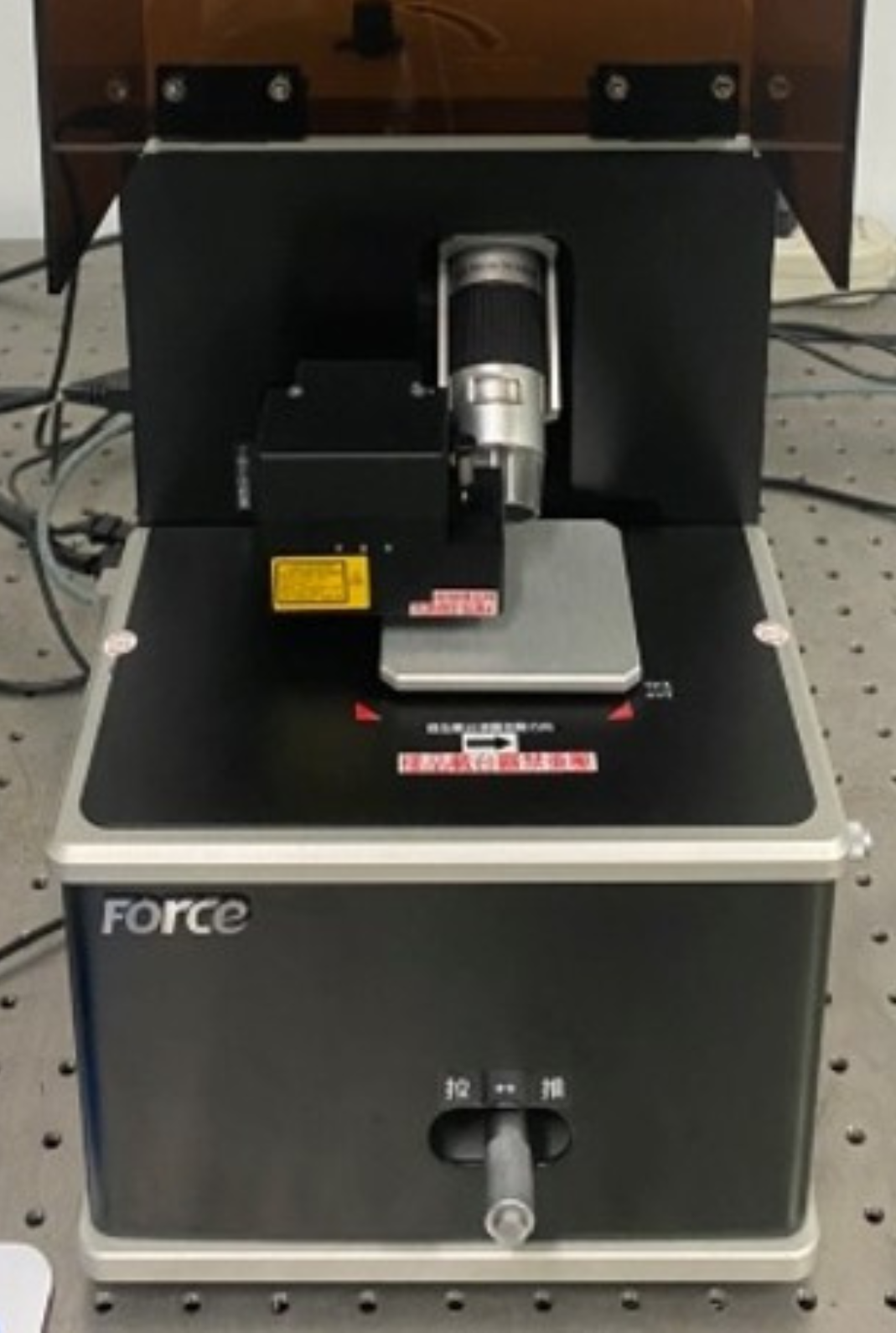
Surface Profiler
Surface Profiler
Instrument Overview

The Surface Profiler (Alpha-Step Profiler) is a high-precision instrument used for measuring thin film thickness and surface topography. The instrument works by scanning the sample surface with a diamond stylus, detecting the stylus's vertical displacement, and converting it into an electronic signal to obtain data on film thickness and surface morphology. This technique is widely used in thin film processing, semiconductor components, and materials engineering fields.
🎯 I. Objective and Applications
-
Thin Film Thickness Measurement
Precise measurement of film thickness at the nano- to micro-meter scale, suitable for post-processing inspection after evaporation, sputtering, etching, and other processes.
-
Surface Profile Analysis
Maps the height variation across the sample surface, used to observe the uniformity and morphological changes in structural layers during processing.
-
Process Quality and Reliability Inspection
Can be used to evaluate thin film stacks, microstructure depth, and pattern morphology to verify process accuracy and stability.
⚙️ II. Principle
-
Probe Scanning
A sharp diamond stylus contacts the sample surface with a controlled force and scans along a specified direction, sensing surface height variations.
-
Signal Recording
The vertical displacement of the stylus is detected and recorded in real-time by a highly sensitive sensor.
-
Signal Conversion & Profiling
The stylus displacement signal is converted into an electronic signal and processed to generate a surface profile plot, which is then used to calculate thin film thickness and morphology distribution.


