




The Chip Journey
The Chip Journey
Before a chip reaches a smartphone, vehicle, or AI server, it travels through design, manufacturing, packaging, and testing.
Every stage matters, and every stage requires professionals with different expertise.
Suggested image: a wafer, packaged chips, a chip cross-section, or a full semiconductor value-chain visual.
Recommended ratio: 16:9
From an Idea to the Technology in Your Hands
Use these four steps to quickly understand the essential stages of the semiconductor value chain.
A chip is not created by one factory or one engineer alone. It is the result of a precise relay among design, materials, processes, packaging, testing, and system applications.
IC Design
Define what the chip needs to do
Wafer Processes
Build microscopic electronic devices
Packaging
Protect and connect the chip
Testing
Verify function, performance, and reliability
Four Key Stages Behind Every Chip
Photo spaces are reserved below. Add authentic equipment, laboratory, or student-practice photos later.
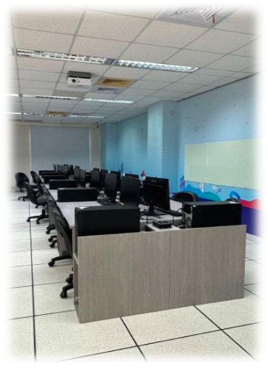
First, Decide What the Chip Should Do
IC design is like creating the blueprint for a highly precise city. Engineers define functions such as computing, memory, image processing, communication, or sensing, and translate them into circuits and system architectures.
This stage involves logical thinking, programming, and circuit concepts. It shows that a chip is not simply small—it is an intelligently designed core.
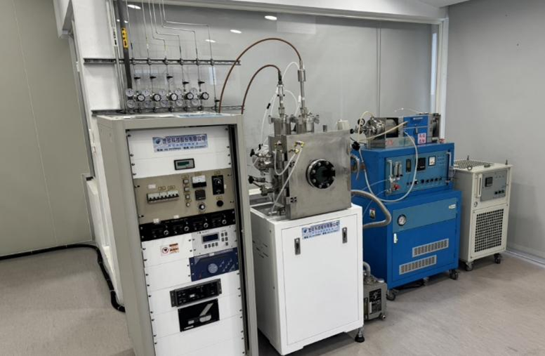
Turn Designs into Microscopic Structures
Wafer processing uses materials, thin films, patterns, and process technologies to gradually form extremely small electronic devices and circuit structures on silicon wafers.
This process demands precision because material variations, process conditions, and surface properties can all affect device performance and quality.
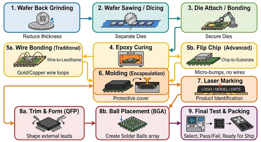
Protect, Connect, and Prepare the Chip for Use
After wafer processing, a chip is still a fragile bare die. Packaging protects it, creates electrical connections, supports heat dissipation, and allows it to communicate with external circuit boards and systems.
Packaging technologies continue to evolve and are increasingly important for improving system performance, reducing product size, and integrating multiple chips.
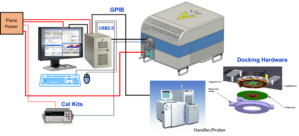
Verify That Every Chip Can Work Reliably
Completed chips undergo measurement, functional testing, and reliability verification to confirm that they meet design requirements and maintain stable performance in different conditions.
Testing and verification are essential quality safeguards, helping technology products enter daily life safely and reliably.
Your Possible Role in This Journey
Semiconductors require diverse talent. You can gradually discover your own place according to your interests.
Design & Systems Thinker
Interested in circuits, programming, logic, and system functions, and enjoys thinking about how chips can complete complex tasks.
Materials & Process Explorer
Interested in materials, chemistry, physics, and precision manufacturing, and enjoys understanding how invisible structures affect chip performance.
Packaging & Integration Practitioner
Enjoys hands-on work and the integration of mechanics and electronics, with interest in chip connection, protection, heat dissipation, and application.
Testing & Quality Gatekeeper
Enjoys measurement, data analysis, and problem solving, helping ensure that chip functions and quality meet requirements.
The Excitement of Semiconductors Is That Every Stage Shapes the Future.
From a design blueprint to a chip that powers the world, every stage requires expertise, patience, and innovation. Continue to the “AU Semiconductor Learning Map” to explore the real learning environments behind this journey.
