



Explore & Experience
Explore & Experience
The best way to explore a field of study is to see it and experience it yourself. Through laboratory visits, cleanroom-attire experiences, process activities, and faculty–student interaction, high-school students can take a closer look at semiconductor engineering.
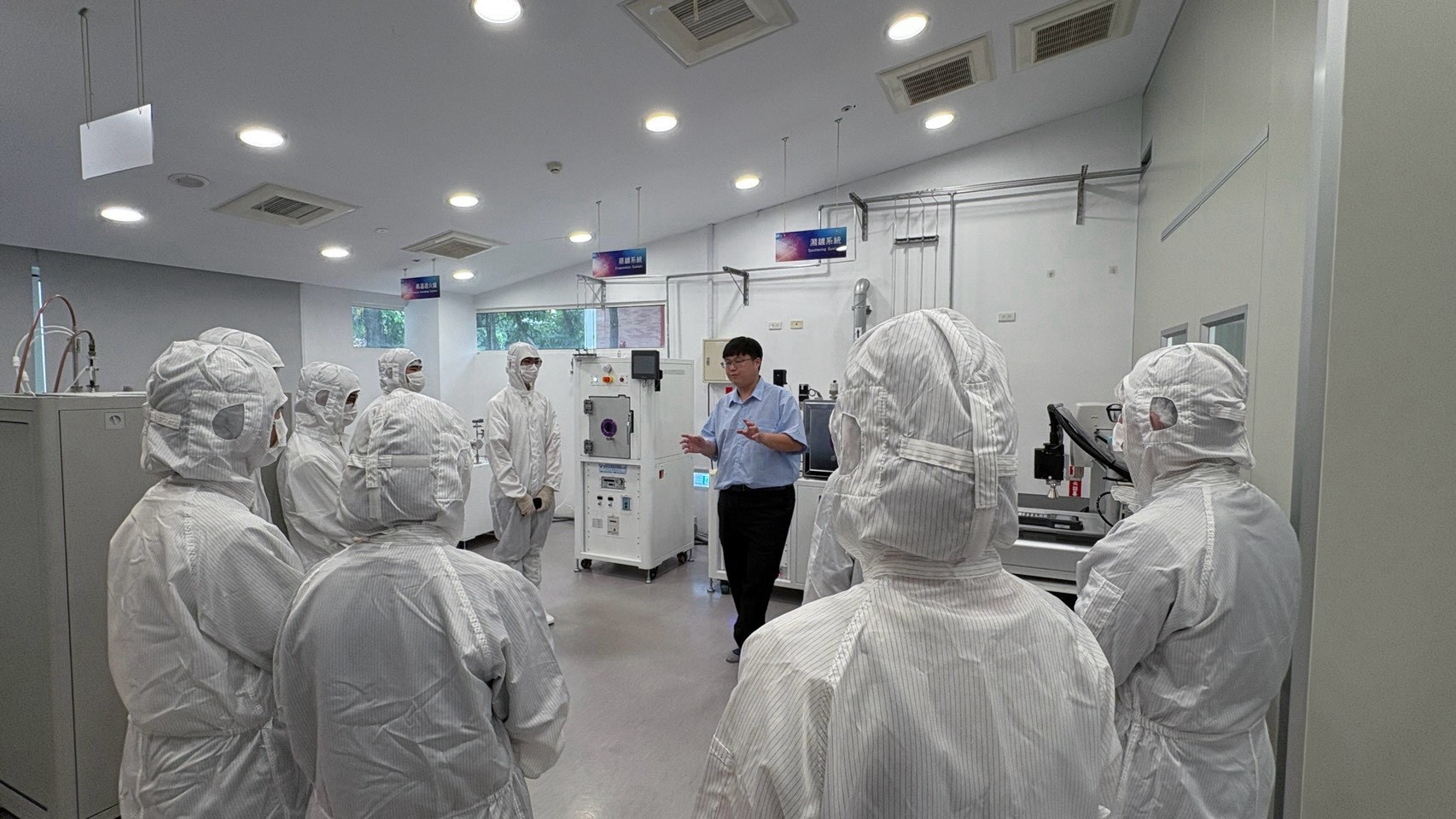
Featured Activity|Semiconductor Engineer Experience Camp
Students began by seeing real facilities and gradually discovered what semiconductor engineering learning looks like.
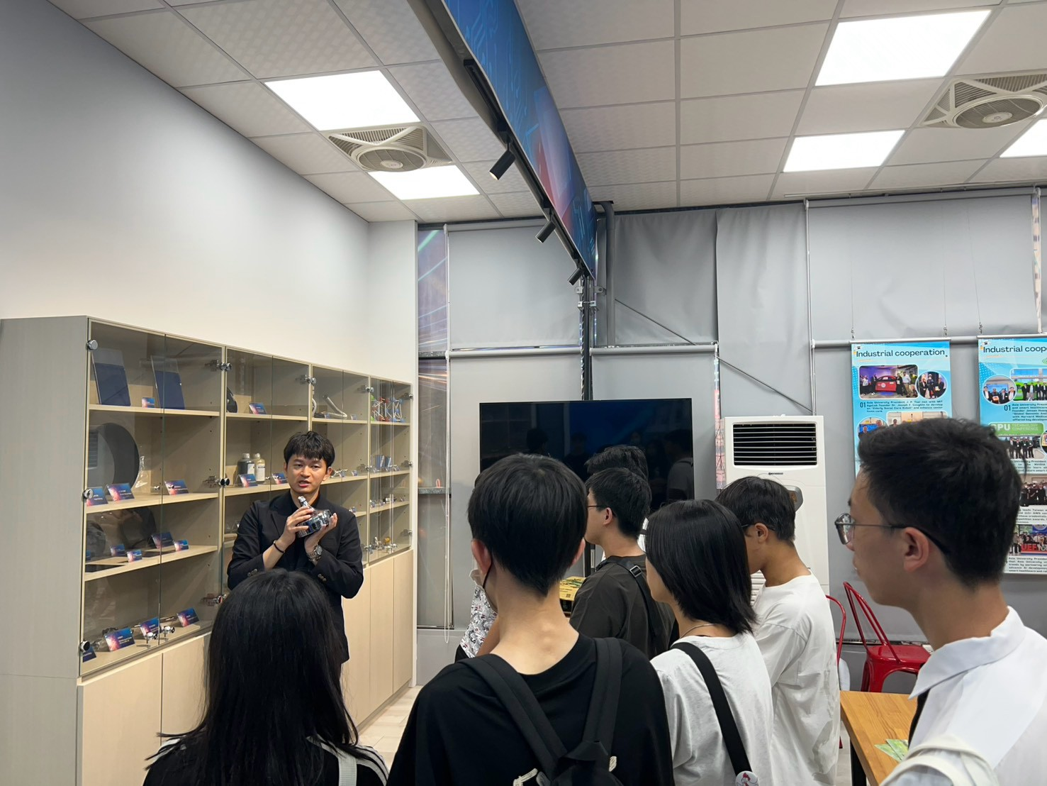
Experience in Action
Every image represents a student’s first step into the world of semiconductors.
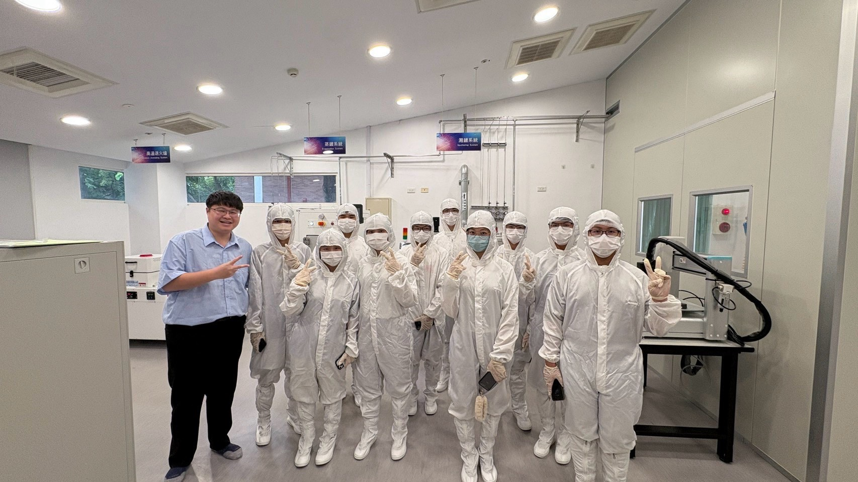 Cleanroom Attire Experience
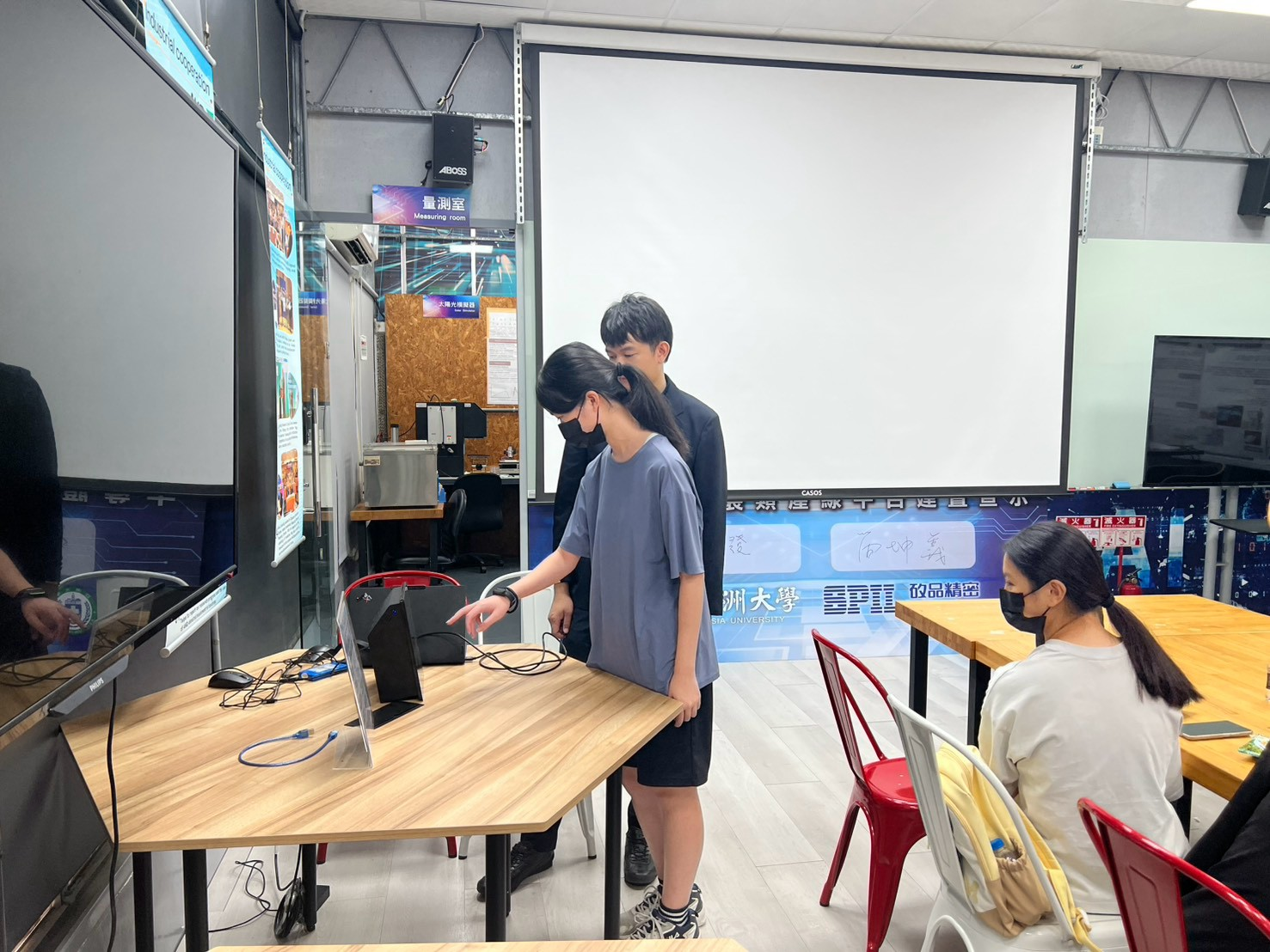 Laboratory & Equipment Tour
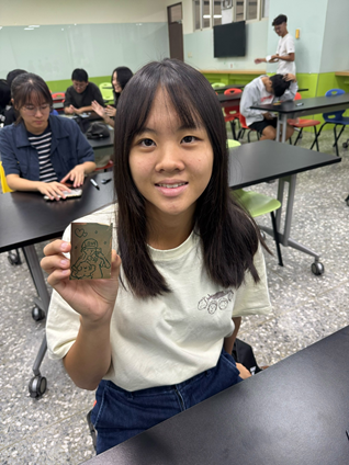 Photolithography Experience
Admissions Activities & Engagement Footprint
Continuing to visit high schools, welcome student groups, and promote international exchange and overseas outreach.
2025–2026 Admissions & Outreach Overview
The program has continued to organize high-school visits, program presentations, experience courses, family engagement, overseas educational outreach, and international exchange activities.
These activities are more than admissions promotion. They help students, families, and teachers better understand the semiconductor industry, learning content, and future development pathways.
High-School Visits Experience Courses Admissions Information International Exchange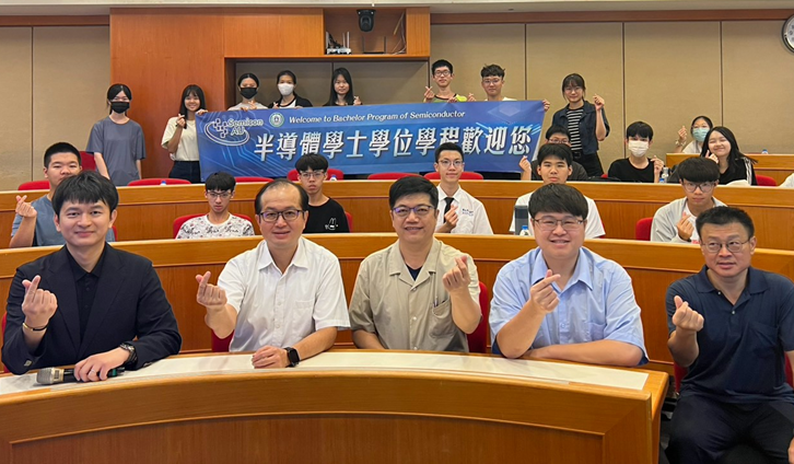
Ways You Can Continue Exploring
Future activity information will be updated through the program’s official website and announcements.
High-School Campus Visits
Faculty-guided visits introduce the program, equipment, and hands-on learning environment while helping students understand the semiconductor value chain.
Semiconductor-Themed Experiences
Explore materials, processes, packaging, testing, and smart technologies through activities designed for high-school students.
Admissions Information & Family Engagement
Help students and families understand admissions pathways, learning content, hands-on resources, and future possibilities.
International Exchange & Outreach
International school exchange and overseas educational outreach allow more students to explore the possibility of studying semiconductors in Taiwan.
Start with One Experience and Discover Your Connection with Semiconductors.
You do not need to be an expert today. By entering the learning environment, asking questions, and exploring with your own hands, you may discover a technology pathway that truly interests you.
