View count:
3667
Research Center
ASIA UNIVERSITY · SEMICONDUCTOR CENTER
Asia University Semiconductor Hands-On Learning Environment
From IC design, materials and devices, processing and measurement, to packaging and testing, Asia University provides diverse learning spaces and practical platforms that make semiconductors more than textbook knowledge—they become an engineering journey that students can see, explore, and understand step by step.
Six Signature Learning Areas
Connecting design, processing, packaging, testing, and collaboration to create a complete semiconductor learning map.
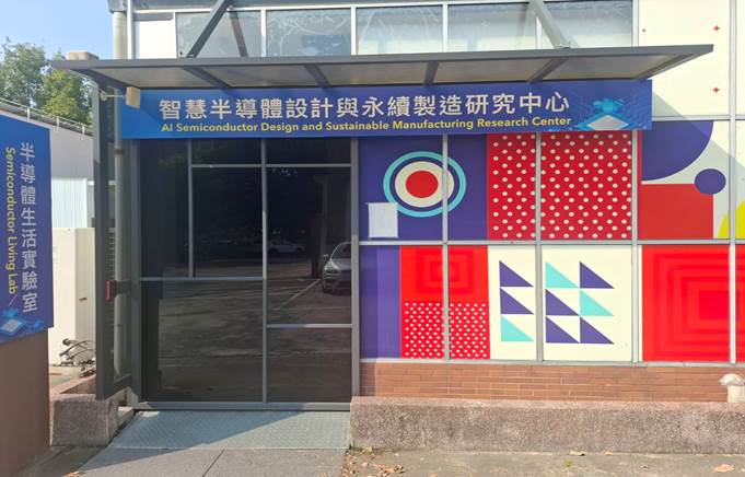
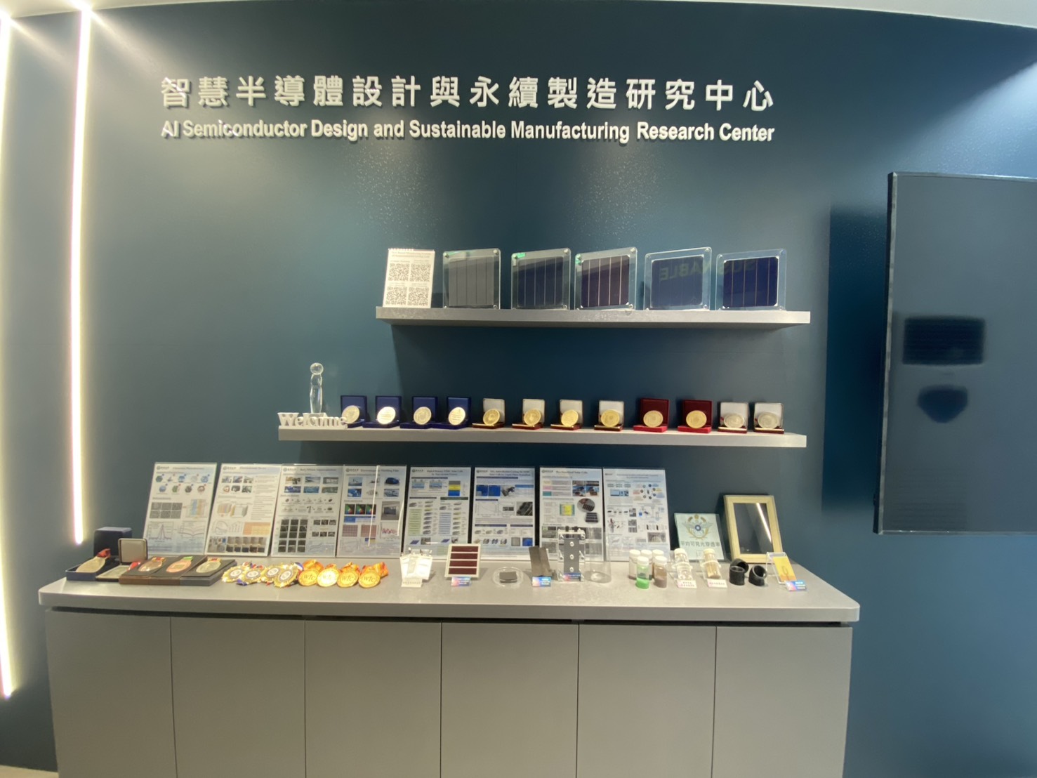
01|DISCUSS & EXPLORE
Semiconductor Learning Studio
A space for student discussion, project collaboration, and independent learning. Through physical displays and interaction, students develop an initial understanding of the semiconductor value chain.
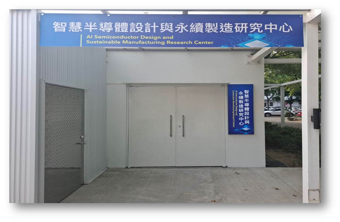
02|RESEARCH & PROCESS
Professional Research Laboratory
Focused on semiconductor process research and practical teaching, the laboratory uses precision instruments and experimental platforms to build students’ observation, operation, and research capabilities.
03|SUSTAINABILITY & EXCHANGE
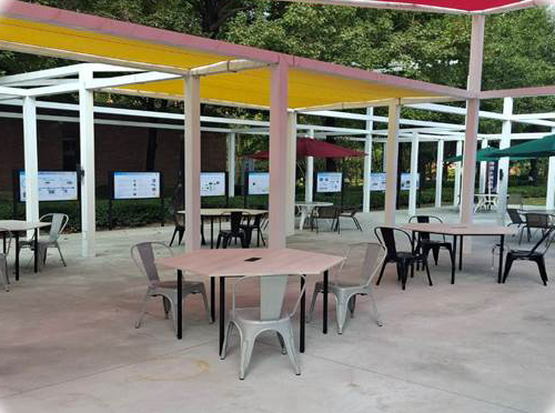
Semiconductor Sustainability Plaza
Combining technology education, sustainability topics, and student interaction, this area extends semiconductor learning into campus life and interdisciplinary dialogue.
04|IC DESIGN
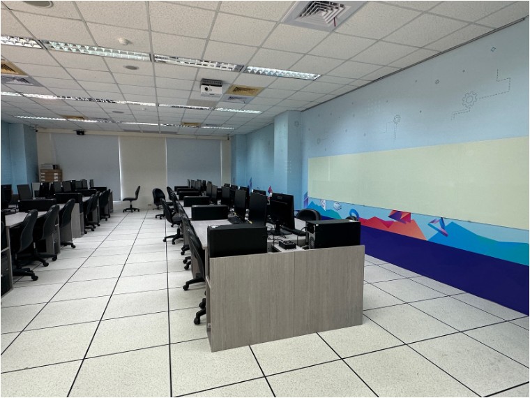
I533 IC Design Classroom
Provides computer workstations and an EDA learning environment for integrated-circuit design, simulation, verification, and related courses—introducing students to the design side of the semiconductor value chain.
05|DEVICE & MEASUREMENT
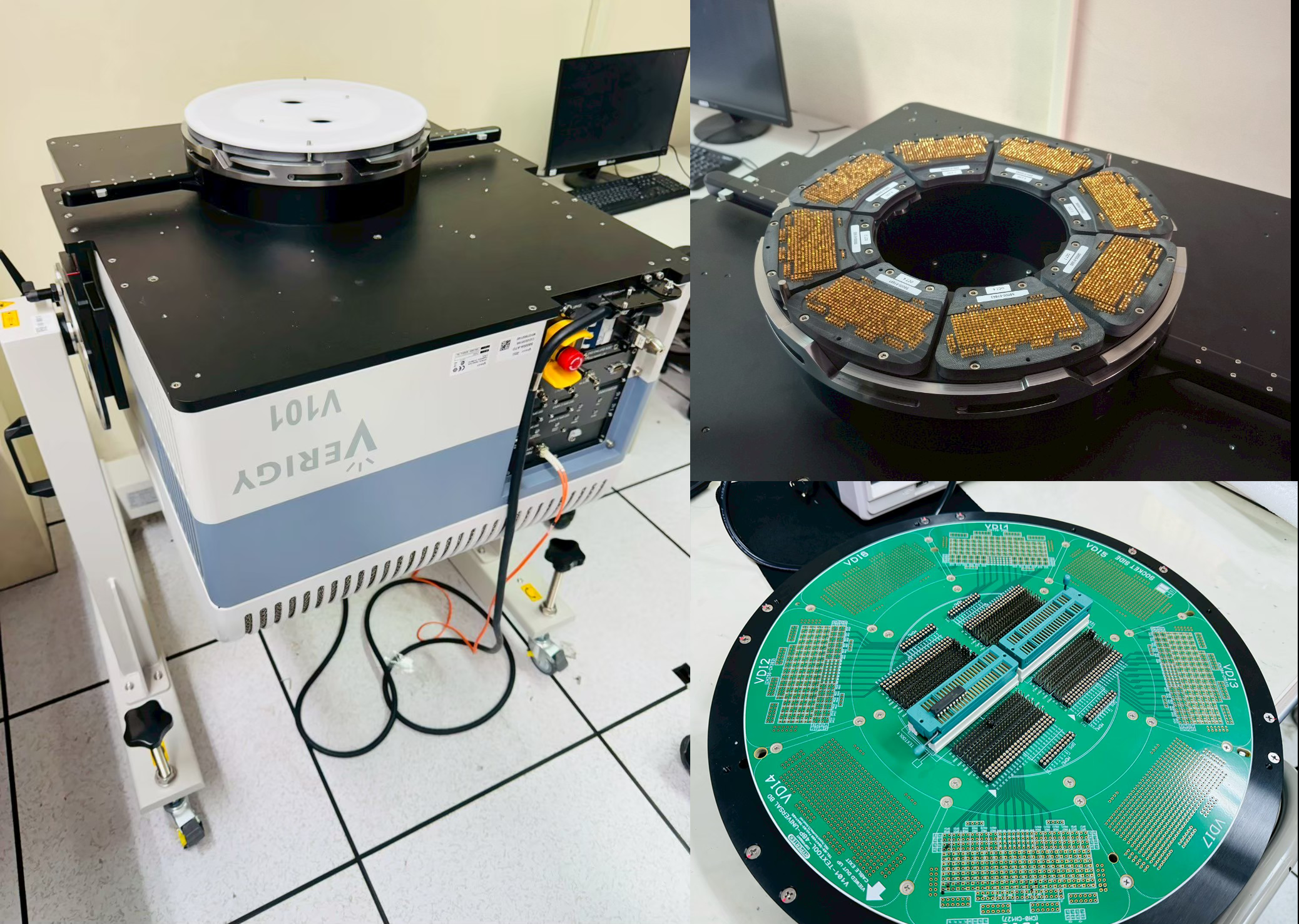
I534 Semiconductor Equipment Laboratory
Focused on semiconductor materials, device physics, basic processes, and electrical measurement, this laboratory helps students turn theoretical knowledge into practical operation and analytical skills.
06|IC PACKAGING
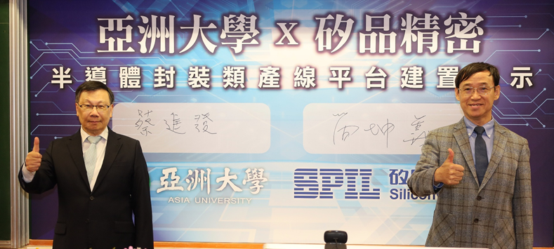
Co-Creating an IC Packaging Quasi Production Line with SPIL
Centered on hands-on packaging education, this platform connects wafer dicing, die attachment, and wire interconnection, helping students understand the real workflow of packaging engineering.
IC Packaging Quasi Production Line|From Die to Package
Using equipment as a learning medium, packaging becomes an engineering process that students can understand and observe.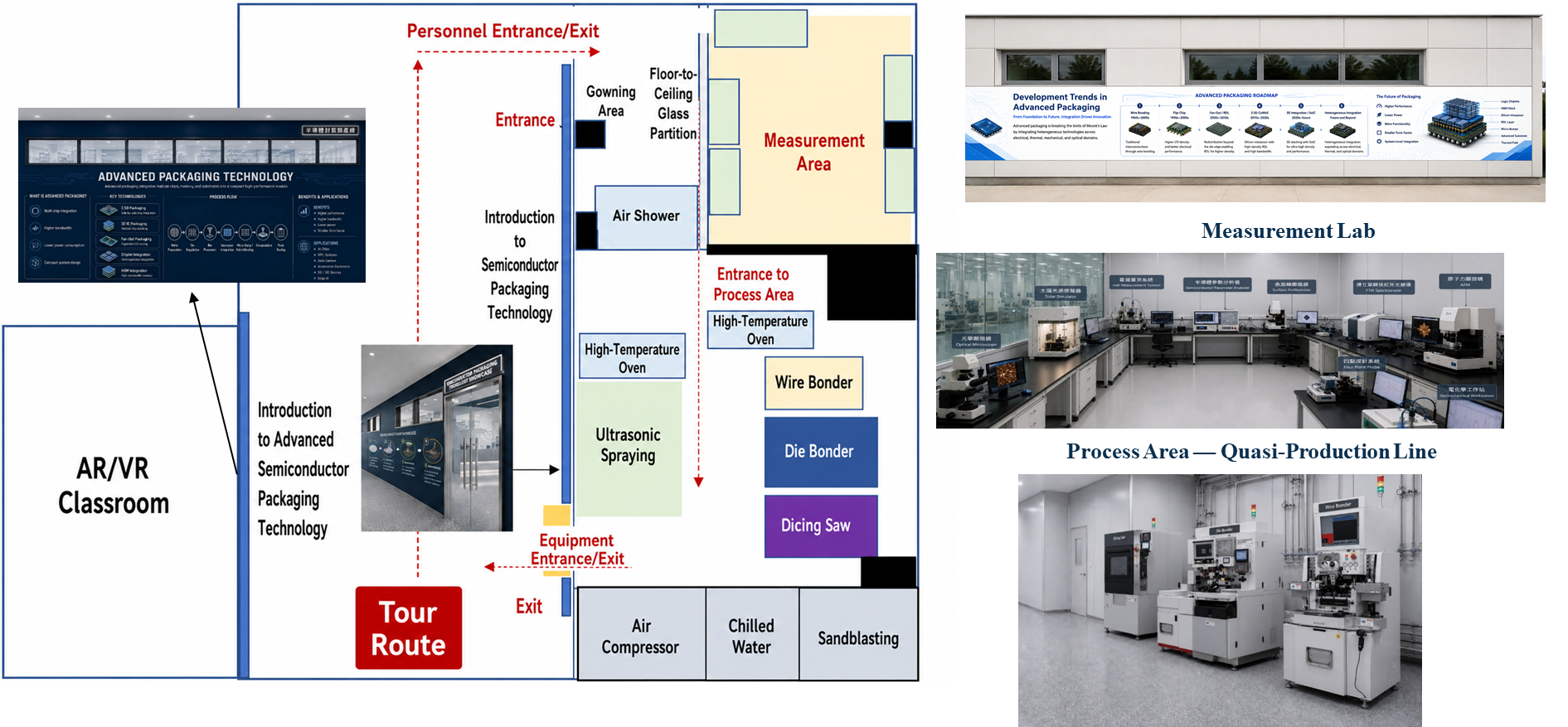
SPIL-SUPPORTED EQUIPMENT · HANDS-ON PACKAGING EDUCATION
Co-Creating a Hands-On Packaging Learning Platform with SPIL
Asia University’s Semiconductor Center has established an IC Packaging Quasi Production Line centered on packaging teaching equipment supported by Siliconware Precision Industries Co., Ltd. (SPIL). The platform helps students understand key packaging stages, including wafer dicing, die attachment, and electrical interconnection.
This is more than an equipment display. It transforms process logic, safety procedures, and quality awareness into learning experiences that students can observe, discuss, and practice.
STEP 01
Dicing Saw|Wafer Dicing
Learn how a wafer is separated along designated scribe lines into individual dies, while understanding the importance of cutting quality, blades, cooling, and safe operation.
STEP 02
Die Bonder|Die Attachment
Understand how a die is precisely attached to a substrate or carrier, and how position, pressure, materials, and process stability affect packaging quality.
STEP 03
Wire Bonder|Wire Interconnection
Learn the basic principle of using fine metal wire to form electrical connections between a die and substrate, including bond quality, wire profile, and reliability concepts.
Learning Value|Turning Process Knowledge into Engineering Capability
Through the IC Packaging Quasi Production Line, students can develop foundational packaging-engineering knowledge through equipment, processes, safety, quality, and teamwork. This platform also connects naturally with learning in materials, processing, measurement, and testing, helping students understand the completeness of the semiconductor value chain.
From Design to Testing: A Connected Learning Map
Through interdisciplinary knowledge, hands-on equipment, and engineering thinking, students develop capabilities for the future semiconductor industry.
IC Design
Design, simulation, and verification
Materials & Devices
Properties, structures, and measurement
Process Integration
Basic processing and engineering thinking
Packaging Practice
Dicing, die attachment, and wire bonding
Testing & Analysis
Measurement, data interpretation, and quality concepts
Asia University · Semiconductor Center · Bachelor Program of Semiconductor