



AU Semiconductor Learning Map
AU Semiconductor Learning Map
From IC design, materials and processes, to packaging and testing, Asia University plans semiconductor learning through a complete value-chain perspective.
Students do more than learn about chips—they explore equipment, laboratories, and hands-on learning environments.
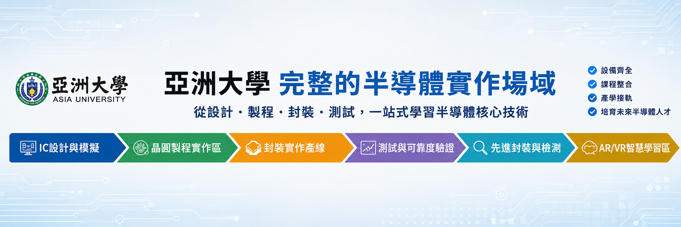
A Complete Semiconductor Learning Pathway
From understanding how chips are designed to exploring how they are manufactured, packaged, and verified.
The Bachelor Program of Semiconductor connects design, processes, packaging, testing, and smart learning, enabling students to build professional foundations and interdisciplinary perspectives through courses, equipment, and hands-on experiences.
Six Hands-on Learning Environments
For each area below, prioritize authentic photos of equipment, faculty guidance, student practice, and visits.
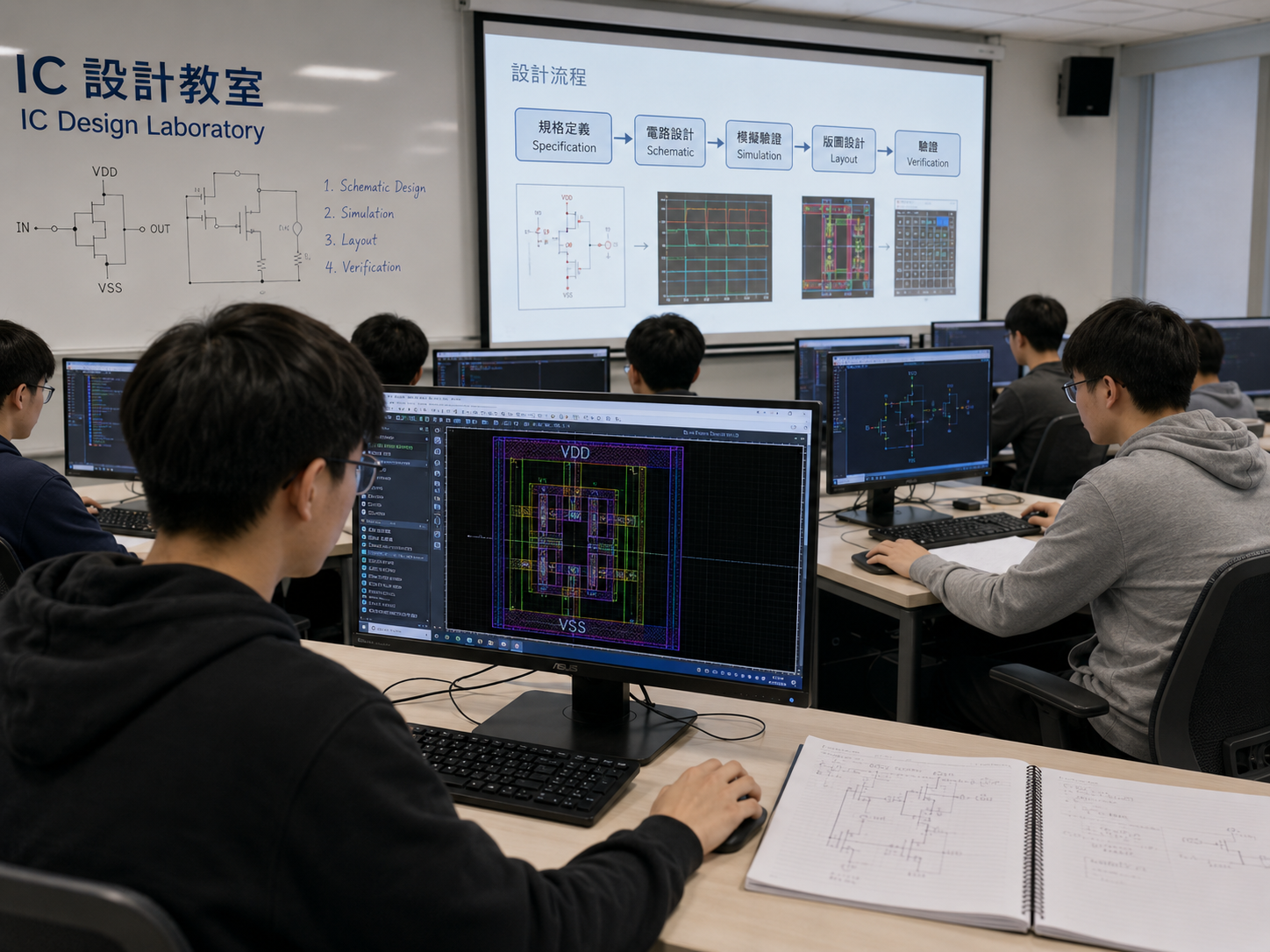
IC Design & Simulation
The chip journey begins with design. Through learning in circuits, devices, and system simulation, students build foundational understanding of chip functions, design logic, and electronic systems.
IC Design Classroom I533 Circuit & System Simulation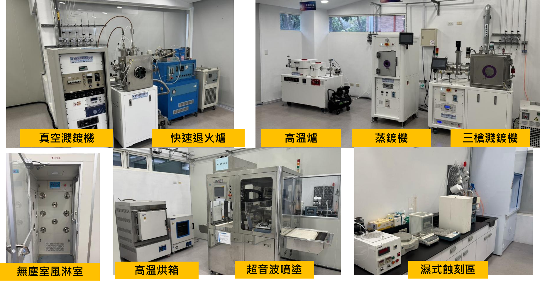
Materials & Wafer Process Learning Area
From material properties, thin films, and process concepts to surface and structural analysis, students learn how semiconductor devices are gradually formed on wafers and how process conditions affect quality and performance.
Semiconductor Equipment Lab I534 Materials Analysis & Measurement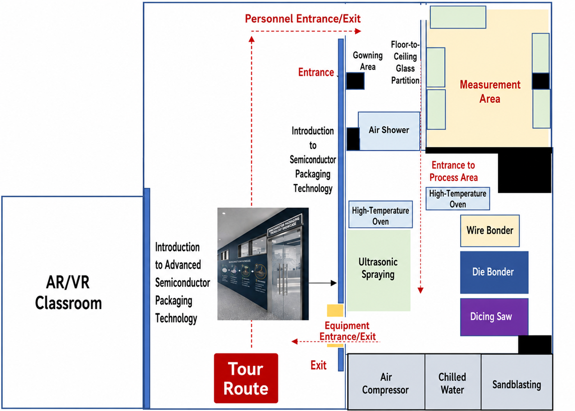
IC Packaging Quasi Production Line
Packaging transforms a fragile bare die into an applicable electronic component. Students explore essential concepts in wafer dicing, die bonding, and wire bonding, and understand how chips are protected, connected, and integrated into systems.
Dicing Saw Die Bonder Wire Bonder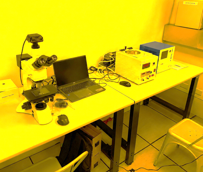
Testing & Reliability Verification
Every chip requires measurement and verification to confirm normal operation. Students learn fundamental concepts in testing, data interpretation, and reliability, and understand how quality is established and protected.
IC Testing Lab V101 Measurement & Data Interpretation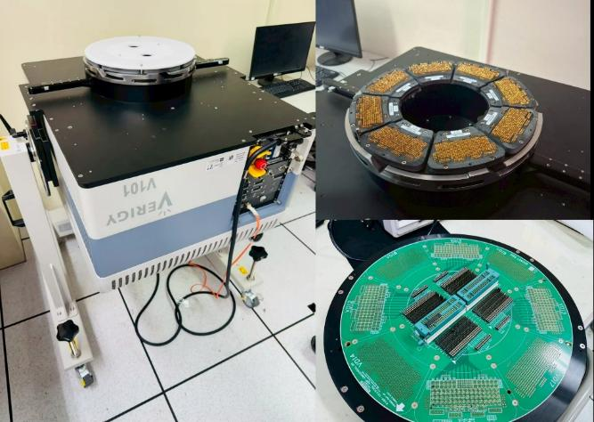
Advanced Packaging & Inspection
As AI, high-performance computing, and smart devices advance rapidly, packaging and inspection are increasingly important. Students explore structures, measurements, and quality concepts to understand the evolution of semiconductor technologies.
Package Structure Learning Inspection & Quality Concepts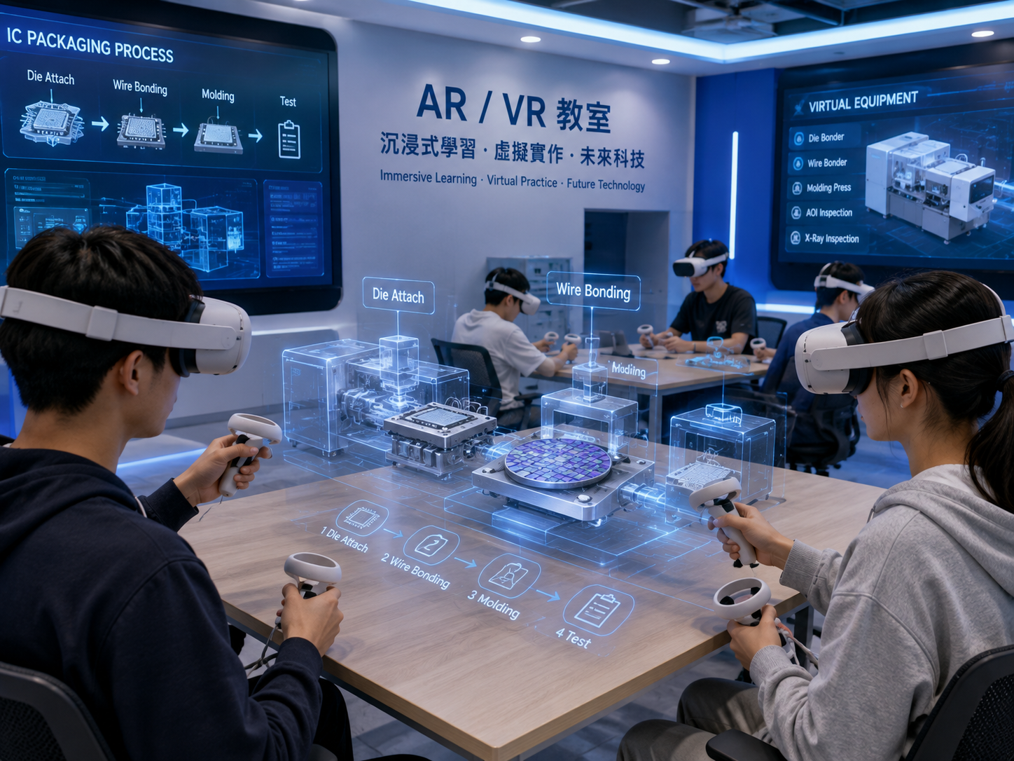
AR/VR Smart Learning Zone
Immersive and interactive learning resources help students understand semiconductor equipment, process steps, and professional environments more intuitively, making complex technology knowledge easier to visualize and explore.
AR/VR Classroom Immersive Technology LearningSee the Equipment. Understand the Industry. Explore the Future.
The value of semiconductor learning at Asia University is not simply introducing technical terms. It helps students understand the role of every piece of equipment, every process step, and every professional capability in the complete semiconductor value chain.
