



Minister of Education CHENG Ying-Yao Visits Asia University
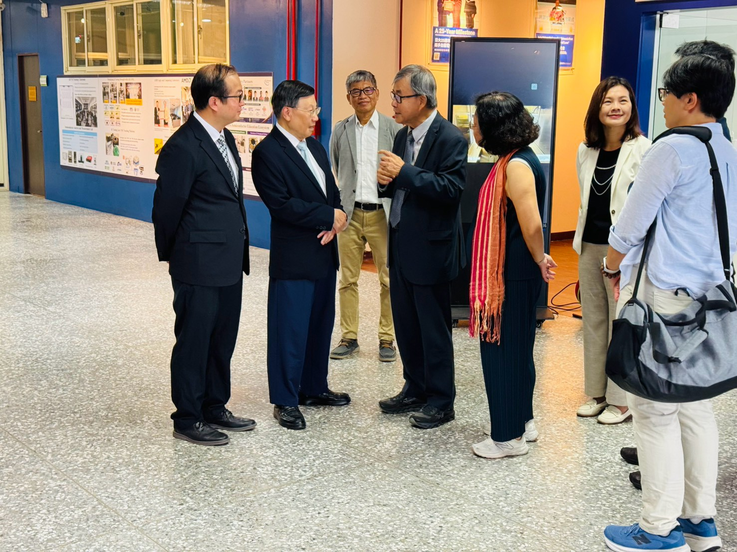 Minister of Education CHENG Ying-Yao (fourth from left), accompanied by Asia University President Jeffrey J. P. Tsai (second from left) and university administrators, visits Asia University’s semiconductor education facilities.
Minister of Education CHENG Ying-Yao visited Asia University on August 13, accompanied by Political Deputy Minister LIU Kuo-Wei and other ministry officials. The delegation toured the University’s semiconductor education and hands-on training facilities to learn about its plans for semiconductor talent development, laboratory infrastructure, practical courses, and industry–academia collaboration. Asia University President Jeffrey J. P. Tsai and university administrators accompanied the delegation and exchanged views with the officials on aligning higher education with the workforce needs of the semiconductor industry.
During the visit, the University introduced its semiconductor fabrication and packaging education facilities. The delegation learned about the instructional applications of photolithography, multilayer exposure, wafer dicing, die bonding, and wire bonding equipment. The University also explained how fabrication principles, equipment operation, and industry practices are incorporated into the curriculum, enabling students to develop a comprehensive understanding extending from theoretical foundations and process operation to semiconductor packaging.
Semiconductor Packaging Quasi-Production Line Developed in Collaboration with SPIL
Asia University has collaborated with Siliconware Precision Industries Co., Ltd. (SPIL) to establish a semiconductor packaging quasi-production line equipped with a wafer dicing saw, die bonder, and wire bonder. The collaboration brings industry-oriented process concepts into hands-on campus instruction. Students can learn the sequential processes of wafer dicing, die pick-and-place and bonding, and gold-wire bonding while developing a practical understanding of equipment operation, process control, and quality requirements.
Asia University President Jeffrey J. P. Tsai stated that the semiconductor industry is strategically important to Taiwan and represents a major priority for talent development in higher education. Asia University continues to integrate its resources in information technology, engineering, and interdisciplinary education while progressively enhancing its semiconductor teaching and research environment. The goal is to equip students not only with fundamental theoretical knowledge but also with an understanding of actual industry processes and technical requirements through equipment operation, project-based learning, and industry collaboration.
PRESIDENT JEFFREY J. P. TSAI“The development of semiconductor education involves more than installing equipment. It requires the integration of curricula, faculty expertise, research, and industry–academia collaboration. The packaging quasi-production line developed with SPIL provides students with a learning environment in which they can experience actual packaging processes. It also serves as an important practical platform connecting university education with industry needs.”
President Tsai added that the University will continue to deepen its engagement with the semiconductor industry and academic institutions in Taiwan and abroad. Through these efforts, Asia University aims to establish a sustainable talent-development mechanism and further strengthen students’ practical capabilities and industry readiness.
An Asia University vice president stated that the University continues to develop practical training in semiconductor fabrication, packaging, and testing in response to educational and workforce-development needs. Through interdisciplinary curricula, facility-based instruction, and industry–academia collaboration, students from different academic backgrounds can gain a broader understanding of the semiconductor value chain. The equipment supports not only classroom instruction but also student projects, faculty research and development, and collaboration with industry.
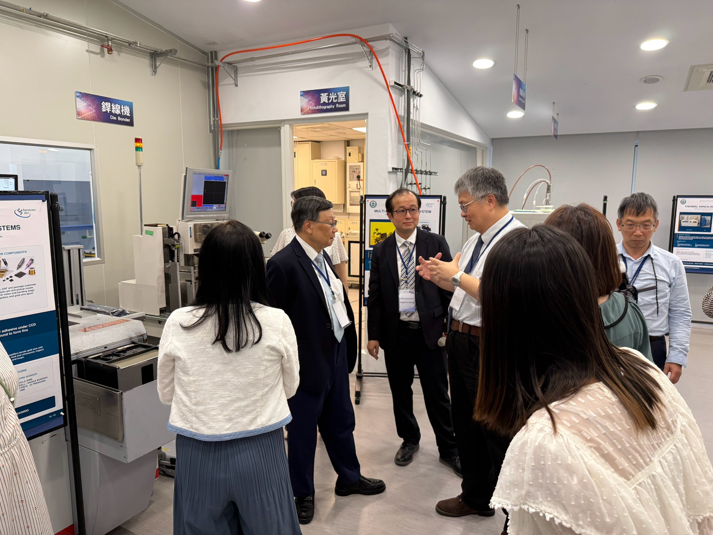
During the visit, Political Deputy Minister LIU Kuo-Wei examined the photolithography, die bonding, and wire bonding facilities and received a briefing on the semiconductor packaging quasi-production line, the development of the instructional facilities, and the associated curriculum. The Ministry of Education delegation and university representatives also exchanged views on equipment utilization, hands-on education, industry–academia collaboration, and semiconductor talent development.
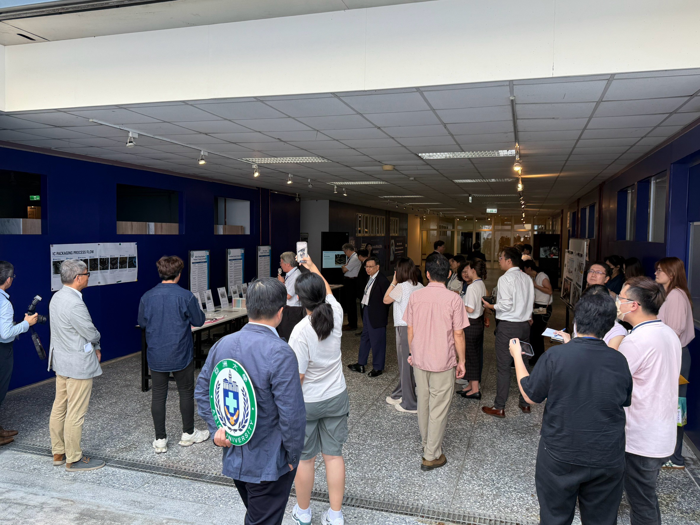
Asia University stated that it will continue to enhance its semiconductor curricula and educational resources, strengthen hands-on training in fabrication, packaging, and testing, and integrate industry collaboration with interdisciplinary research. Through these efforts, the University is progressively developing a semiconductor talent-development environment that connects education, research, and industry needs.
Visit Highlights
- Minister of Education CHENG Ying-Yao, Political Deputy Minister LIU Kuo-Wei, and other ministry officials visited Asia University.
- The delegation toured the University’s photolithography, multilayer exposure, and semiconductor fabrication education facilities.
- The delegation visited the semiconductor packaging quasi-production line developed by Asia University in collaboration with SPIL.
- Officials learned about hands-on training in wafer dicing, die bonding, and wire bonding.
- Ministry and university representatives exchanged views on semiconductor talent development, practical education, and industry–academia collaboration.
